
Introduction: Why PCB Design is the Foundation of Reliable IoT Products
In the world of IoT product development, the printed circuit board (PCB) is more than just a substrate for components—it’s the physical manifestation of your entire system architecture. A well-designed PCB directly determines whether your IoT device will function reliably in diverse environments, meet regulatory requirements, achieve promised battery life, and scale cost-effectively to production.
Consider this: approximately 40% of IoT product failures trace back to PCB design issues—unexpected power consumption, electromagnetic interference, manufacturing defects, or environmental vulnerabilities. The difference between a prototype that works on your desk and a production-ready product lies in how you approach PCB design from day one.
Prototype PCBs are about proving functionality: can we make it work once?
Production PCBs are about ensuring reliability: will it work consistently for thousands of devices across different environments while meeting cost targets and certification requirements?
This article focuses on bridging that gap, providing practical PCB design fundamentals specifically for IoT product developers who need to move from concept to scalable product.

Ready to see where PCB design fits into the bigger picture of building a successful connected product? Mastering hardware fundamentals is just one essential piece of the Complete IoT Product Development Skill Ecosystem. Our pillar article, The Complete IoT Product Development Skill Ecosystem: From Idea to Scale, maps out the entire journey from concept to deployment, detailing how hardware design intersects with firmware, cloud development, security, and product strategy. It’s the perfect guide to understand how your PCB expertise integrates with the other critical disciplines needed to bring a reliable, scalable IoT product to market.
Understanding IoT-Specific PCB Design Requirements
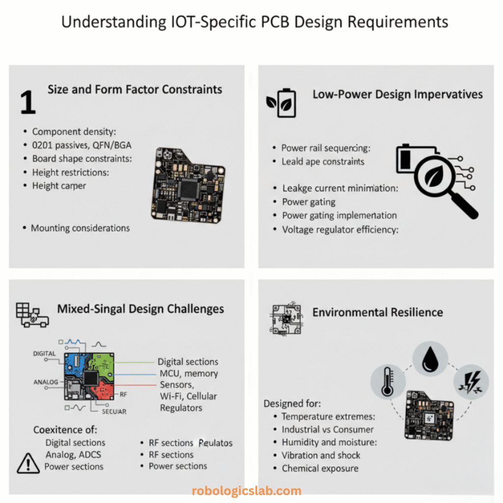
Size and Form Factor Constraints
IoT devices often need to fit into compact spaces—wearables, sensors embedded in equipment, consumer devices with sleek designs. This imposes strict constraints:
- Component density: Smaller packages (0201, 01005 passives, QFN/BGA ICs)
- Board shape constraints: Irregular shapes to fit enclosures
- Height restrictions: Components must fit within specified Z-heights
- Mounting considerations: Board-to-enclosure mounting points and clearances
Low-Power Design Imperatives
Battery-operated IoT devices demand exceptional power management at the PCB level:
- Power rail sequencing: Proper startup/shutdown sequences for multiple voltage domains
- Leakage current minimization: High-impedance circuit design
- Power gating implementation: MOSFETs for disabling unused subsystems
- Voltage regulator efficiency: LDO vs switching regulator selection based on load profiles
Mixed-Signal Design Challenges
IoT PCBs typically combine:
- Digital sections: MCU, memory, digital interfaces
- Analog sections: Sensors, ADCs, audio circuits
- RF sections: Wi-Fi, Bluetooth, cellular, LoRa modules
- Power sections: Switching regulators, battery management
Each domain has different layout requirements and noise sensitivities that must coexist peacefully.
Environmental Resilience
IoT devices operate in diverse environments:
- Temperature extremes: Industrial (-40°C to +85°C) vs consumer (0°C to +70°C)
- Humidity and moisture: Conformal coating requirements
- Vibration and shock: Component securing and strain relief
- Chemical exposure: Industrial or automotive applications
Schematic Capture: Translating System Requirements into Reality
Power Architecture Planning
Your power architecture schematic defines battery life and reliability:
[Example IoT Power Tree]
Battery → Protection Circuit → Buck Converter (3.3V) → LDO (1.8V) → Core
                               ↓
                            LDO (3.0V) → RF Module
                               ↓
                            Sensor Power (Gated)
Key considerations:
- Efficiency at expected load currents: Switching regulators lose efficiency at light loads
- Transient response: Can regulators handle sudden current demands from RF transmission?
- Power sequencing: Some ICs require specific power-up sequences
- Battery protection: Overcharge, over-discharge, and short-circuit protection
MCU/SoC Selection and Peripheral Interfacing
When placing your MCU on the schematic:
- Decoupling strategy: Multiple capacitors at different frequencies (100µF + 10µF + 0.1µF + 0.01µF pattern)
- Crystal oscillator circuit: Proper load capacitors and grounding
- Debug interfaces: SWD/JTAG with proper series resistors
- Unused pin handling: Configure as outputs or with pull-up/pull-down resistors
- ESD protection: TVS diodes on external interfaces
Sensor and Communication Module Integration
Common schematic mistakes to avoid:
- I²C bus issues: Missing pull-up resistors or incorrect values
- SPI signal integrity: Improper termination for longer traces
- Analog sensor interfaces: Incorrect filtering or bias circuits
- RF module connections: Impedance-controlled traces from day one
Reference Designs: Your Best Starting Point
Always begin with the manufacturer’s reference design, but understand why each component exists:
- Evaluation boards: Show ideal layout but may omit cost-optimized components
- Application notes: Provide critical design insights for specific use cases
- Errata sheets: List known silicon issues and workarounds
As an engineer crafting robust IoT hardware, the ability to decipher a technical datasheet is a non-negotiable skill, transforming a daunting document into a design blueprint. For a deep dive into this essential competency, I highly recommend the comprehensive guide, “How-To: Read and Understand Technical Datasheets”, published by DigiKey’s Maker.io staff. This excellent resource breaks down the anatomy of a datasheet, teaching you how to efficiently navigate from the high-level summary on the first page to the critical details like absolute maximum ratings, pin configurations, and timing diagrams. It provides practical strategies for interpreting truth tables for digital components and leveraging performance graphs to understand how factors like temperature affect your chosen part. Mastering the systematic approach outlined in this tutorial will empower you to select components confidently, ensure they operate within safe limits, and implement them correctly on your PCB, directly increasing the reliability and resilience of your IoT product designs. You can find this invaluable guide here: How-To: Read and Understand Technical Datasheets.
Component Selection: Balancing Performance, Cost, and Availability
Selection Criteria Matrix
Create a spreadsheet comparing components across:
- Power consumption (active, sleep, shutdown currents)
- Cost (unit price at 1K, 10K, 100K quantities)
- Availability (lead time, multiple sources, lifecycle status)
- Package (ease of assembly, thermal performance)
- Performance (specification margins for your application)
MCU Selection Considerations
Beyond MHz and memory:
- Wake-up sources and latency: Critical for low-power applications
- Peripheral availability: Avoid “GPIO starvation” in compact designs
- Power domains: Can unused peripherals be completely powered down?
- Package options: QFN vs BGA vs QFP for prototyping vs production
RF Module Decisions
Integrated module vs discrete design:
Integrated Module Pros:
- Pre-certified (FCC, CE, etc.)
- Faster time-to-market
- Known performance

Discrete RF Pros:
- Lower unit cost at scale
- Custom antenna optimization
- Size optimization possible
Passive Component Selection
Often overlooked but critical:
- Capacitors: X7R/X5R for decoupling, C0G/NP0 for timing circuits
- Resistors: 1% tolerance for precision circuits, watch power ratings
- Inductors: Saturation current rating for switching regulators
- Crystal vs oscillator: Stability vs cost and board space trade-offs
Footprint Accuracy: The Hidden Manufacturing Killer
Component libraries must be accurate:
- Pad dimensions: Too small causes solder voids, too large causes bridging
- Courtyard areas: Ensure clearance for pick-and-place machines
- Polarity markings: Clear and visible for assembly technicians
- 3D models: Essential for enclosure fit checks
PCB Layout Fundamentals for IoT Devices
Layer Stack-up Strategy
2-layer boards (for simple, cost-sensitive designs):
- Limited routing space, challenging ground return paths
- Use ground grid pattern rather than attempting a ground plane
- Route critical signals first, power second
4-layer boards (recommended for most IoT products):
Typical stack-up:
Top Layer: Components, signals
Inner Layer 1: Ground plane (solid)
Inner Layer 2: Power planes (split)
Bottom Layer: Signals, some components
Advantages: Controlled impedance, better EMI performance, easier routing
6+ layer boards: For complex designs with multiple power domains or high-speed interfaces
Grounding Strategy: The Foundation of Signal Integrity
Single-point vs multi-point grounding:
- Single-point: Best for low-frequency analog circuits
- Multi-point: Essential for mixed-signal and RF designs
Ground plane best practices:
- Keep ground planes continuous (avoid splits when possible)
- Use multiple vias for ground connections (reduces inductance)
- Separate analog and digital grounds but connect at a single point near the ADC
Power Distribution Network (PDN) Design
A robust PDN prevents voltage droop during RF transmission or MCU wake-up:
- Power plane strategy: Solid planes for core voltages, pours for others
- Decoupling capacitor placement:
- Place smallest capacitors closest to power pins
- Multiple vias from capacitor pads to ground/power planes
- Don’t daisy-chain decoupling capacitors
- Trace sizing: Use PDN calculators for current capacity and voltage drop
Signal Integrity Basics
For typical IoT clock speeds (<100MHz), focus on:
- Controlled impedance: Only critical for RF lines and high-speed interfaces (USB, MIPI)
- Trace length matching: Important for differential pairs (USB, Ethernet) and DDR memory
- Via count minimization: Each via adds inductance and potential impedance discontinuity
Clock Routing
- Route clock signals first and directly
- Keep away from noisy circuits (switching regulators, digital buses)
- Ground guard traces on both sides
- Minimize vias (ideally zero)
EMI/EMC-Aware PCB Layout: Passing Certification
Understanding EMI Sources in IoT Devices
Primary noise sources:
- Switching regulators: Fast edges generate broadband noise
- Digital circuits: Clock harmonics
- RF transmitters: Fundamental and harmonic emissions
- Improper return paths: Ground bounce and common-mode currents
RF Module Placement and Antenna Considerations
- Antenna clearance: Maintain keep-out areas per module manufacturer specifications
- Ground plane effects: Antennas require proper ground plane dimensions
- Component placement: Keep all components away from antenna area
- RF trace routing: 50Ω impedance control, minimal length, no vias if possible
High-Speed and Switching Noise Management
Switching regulator layout checklist:
- Keep input and output capacitor loops small
- Place inductor close to switching node
- Use ground plane under regulator (not split)
- Route feedback away from noisy areas
Digital noise containment:
- Series resistors on clock lines to reduce edge rates
- Proper bus termination
- Local decoupling at every IC
Section Separation: Analog, Digital, RF
Physical separation with “moats”:
[Board Layout Example]
┌─────────────────────────────────┐
│         RF Section              │
│   Antenna    RF Module          │
│                                 │
│═════════════════════════════════│ ← Ground stitch vias
│                                 │
│      Analog Section             │
│   Sensors  ADC  Filtering       │
│                                 │
│═════════════════════════════════│ ← Single ground connection point
│                                 │
│     Digital Section             │
│   MCU    Memory   USB           │
│                                 │
│   Power Section                 │
│   Regulators  Battery Connector │
└─────────────────────────────────┘
EMC Testing Preparation
Design with testing in mind:
- Test points: Provide for conducted emissions measurements
- Shielding provisions: Include pads for shielding cans if needed
- Filter placement: Position EMI filters at cable entry points
- Grounding studs: For chassis grounding if required
Designing for Manufacturability (DFM): From Design to Volume Production
PCB Fabrication Constraints
Communicate clearly with your fabricator:
- Minimum trace/space: Typically 4/4 mil for standard processes
- Annular ring: Ensure sufficient copper around vias
- Via size and plating: Aspect ratio limitations
- Copper weight: 1oz standard, 2oz for high current
Solder Mask and Silkscreen Guidelines
- Solder mask expansion: Typically 0.1mm beyond pads
- Silkscreen legibility: Minimum text height 0.8mm, line width 0.15mm
- Polarity markings: Clear and consistent orientation
- Pin 1 indicators: On all ICs and connectors
Assembly Considerations
For automated assembly:
- Fiducial marks (at least 3, preferably on opposite corners)
- Component-to-board-edge clearance (typically 3mm)
- Avoid placing components on both sides if possible
- Consistent component orientation for pick-and-place
For rework and repair:
- Adequate space for soldering iron or hot air nozzle
- Test points for critical signals
- Avoid placing tall components near fine-pitch ICs
Panelization for Volume Production
- Tab routing vs V-scoring: Based on board shape and thickness
- Tooling holes: For alignment during assembly
- Breakaway tabs: Size and placement for clean separation
- Test coupons: Include in panel for fabricator process control
Cost Optimization Techniques
- Reduce layer count when possible
- Standardize hole sizes (fewer drill bit changes)
- Minimize board size without compromising layout
- Use standard materials (FR-4 standard Tg)
- Design for common panel sizes (reduce material waste)
Prototyping vs Production PCB Design
Prototype Design Philosophy
- Test points everywhere: Easier debugging
- Optional components: Provision for different configurations
- Larger components: Easier hand assembly and rework
- Extra headers: For measurement and external connections
Transitioning to Production
Design changes typically needed:
- Component consolidation: Replace multiple discretes with integrated solutions
- Size reduction: Optimize layout, remove debug features
- Cost reduction: Alternative components, layer reduction
- Manufacturability improvements: Adjust to assembly house capabilities
- Testability additions: Bed-of-nails test points, JTAG boundary scan
Cost Optimization at Scale
- Value engineering: Regular component reviews as volumes increase
- Second sourcing: Qualify alternate components early
- Design for automation: Eliminate manual assembly steps
- Standardization: Reuse proven circuit blocks across products
Testing and Debug Provisions
Even in production designs, include:
- Programming headers: For firmware updates in the field
- Critical signal test points: Under components if necessary
- Current measurement points: Series 0Ω resistors for profiling
- Factory test interfaces: For production line testing
Tools and Workflow for IoT PCB Design
Tool Selection
Open source options:
- KiCad: Full-featured, excellent for startups and hobbyists
- LibrePCB: Modern architecture, good library management
Commercial options:
- Altium Designer: Industry standard, excellent for complex designs
- Autodesk Eagle: Good for smaller boards, integration with Fusion 360
- Cadence OrCAD/Allegro: Enterprise-level, steep learning curve
Online platforms:
- EasyEDA: Browser-based, integrated with JLCPCB assembly service
Design Workflow Best Practices
- Schematic review before starting layout
- Board outline and mounting holes first
- Component placement with mechanical constraints
- Critical routing (clocks, RF, differential pairs)
- Power distribution routing
- Remaining signal routing
- Design rule check (DRC) and electrical rule check (ERC)
- 3D model export for enclosure verification
- Design review with team members
- Gerber generation with fabrication notes
Version Control for Hardware
Treat PCB designs like software:
- Git for binary files: Use Git-LFS or similar for schematic/layout files
- Meaningful commit messages: Document design decisions
- Branching strategy: Features, revisions, production variants
- Bill of Materials (BOM) management: Track component changes
Real-World Example: ESP32-Based Environmental Sensor PCB
Let’s walk through key design decisions for a production-ready environmental sensor (ESP32 + BME280 sensor + battery management):
Schematic Decisions
- Power section:
- TP4056 lithium battery charger with protection
- TPS63001 buck-boost converter (handles 2.8V-4.2V battery range)
- Separate LDO for analog sensor power
- ESP32 connections:
- External SPI flash for additional storage
- All GPIO broken out to headers for future expansion
- UART-to-USB chip for programming and debugging
- Sensor interface:
- BME280 on I²C with independent power control
- Additional I²C header for other sensors
- Proper pull-up resistors calculated for bus capacitance
Layout Implementation
4-layer stack-up:
- Top: Components, RF traces
- Inner1: Solid ground
- Inner2: 3.3V and battery power planes
- Bottom: Additional components, routing
RF section:
- PCB antenna with proper ground clearance
- All components removed from antenna zone
- Shield can over ESP32 RF section
Power distribution:
- Star topology from battery input
- Bulk capacitors at regulator inputs/outputs
- High-current traces widened appropriately
Manufacturing considerations:
- All components on top side only
- 0603 passives for easy assembly
- Test points for battery current measurement
- Fiducials in three corners
Skill Development Path for PCB Designers in IoT
Beginner Stage (0-6 months)
Focus: Fundamentals and simple boards
- Learn schematic capture with simple circuits
- Master component library creation
- Design single-layer or two-layer boards
- Understand basic design rules
- Build and debug first prototypes
Projects: Arduino shields, simple sensor boards, power supply modules
Intermediate Stage (6-18 months)
Focus: Mixed-signal and RF-aware design
- Design 4-layer boards with controlled impedance
- Implement proper grounding strategies
- Work with RF modules and antennas
- Understand EMI reduction techniques
- Collaborate with mechanical engineers on enclosures
Projects: Bluetooth sensor nodes, Wi-connected devices, battery-powered products
Advanced Stage (18+ months)
Focus: Production-ready designs and system integration
- Design for high-volume manufacturing
- Manage complete product development cycle
- Coordinate with firmware teams on debug interfaces
- Optimize for cost and reliability
- Lead design reviews and mentorship
Projects: Commercially deployed IoT products, complex multi-board systems
Learning Approach Recommendations
- Start with existing designs: Modify proven boards to understand decisions
- Build everything you design: Debugging reveals layout flaws
- Learn measurement techniques: Oscilloscope, spectrum analyzer, vector network analyzer
- Study failed designs: Analyze what went wrong in others’ projects
- Stay current with technology: New components and manufacturing capabilities
Integration with Other Disciplines
PCB designers must collaborate with:
- Firmware engineers: Debug interfaces, boot mode configurations
- Mechanical engineers: Enclosure fit, thermal management, mounting
- RF engineers: Antenna performance, shielding requirements
- Test engineers: Production test points, fixture design
- Supply chain: Component availability, second sourcing
Conclusion: PCB Design as a Core IoT Competency
Quality PCB design is not an optional specialization in IoT product development—it’s a fundamental skill that directly impacts every aspect of your product’s success. From battery life to reliability, from certification to manufacturing cost, the decisions made during PCB design echo throughout the product lifecycle.
The journey from prototype to production-ready PCB involves:
- Shifting mindset from functionality to reliability
- Mastering mixed-signal layout for noise-sensitive IoT applications
- Designing for manufacturability from the earliest stages
- Validating through measurement not just simulation
- Iterating based on real-world performance in target environments
As IoT continues to evolve with edge AI, higher integration, and more challenging environments, PCB design skills will only become more critical. The best IoT developers understand that the physical implementation—the PCB—is where theoretical designs meet reality, and where product success is ultimately determined.
Remember: Every IoT product that succeeds in the market does so on a foundation of well-designed, reliable, manufacturable PCBs. Your journey to mastering this skill begins with your next board design—approach it with production in mind from the very first component placement.
[Internal link back to pillar article: “The Complete IoT Product Development Skill Ecosystem”]
[Teaser: Coming next in our hardware series: “Power Management Design for Battery-Powered IoT Devices” and “RF Implementation Strategies f
FAQs on PCB Design for IoT Devices
1. What’s the most important first step when starting a new IoT PCB design?
Answer:
Define clear design requirements before touching any CAD tool. Create a “design constraints document” that specifies:
- Power budget (battery life targets, sleep/active currents)
- Size and form factor (including height restrictions)
- Environmental conditions (temperature range, humidity, vibration)
- Connectivity requirements (Wi-Fi, Bluetooth, cellular)
- Certification needs (FCC, CE, industry-specific)
- Cost targets (BOM cost, assembly cost)
- Manufacturing volume (prototype vs. mass production)
Without these parameters, you’ll waste time redesigning. For example, choosing components before knowing your operating temperature range could lead to failures in the field. Documenting requirements upfront ensures all team members work toward the same goals.
[Internal link: “Creating Effective IoT Product Requirements Documents”]
2. When should I use a 2-layer vs. 4-layer PCB for IoT devices?
Answer:
Use this decision matrix:
| Choose 2-layer if: | Choose 4-layer if: |
|---|---|
| Extremely cost-sensitive (consumer products <$5 BOM) | Mixed-signal design (analog sensors + digital processing) |
| Low-frequency only (<10MHz) | RF circuits (Wi-Fi, Bluetooth, cellular) |
| Simple power requirements (single voltage) | Multiple power domains (core, I/O, analog) |
| Large board size available | Size-constrained design |
| Prototype phase only | Production design |
| No EMI/EMC certification needed | Must pass FCC/CE certification |
Rule of thumb: Start with 4-layer for any connected IoT device. The additional cost (~$50-100 more for prototypes, ~$0.50-2.00 more in volume) is worth it for better EMI performance, easier routing, and higher first-pass success rate. You can downgrade to 2-layer during cost-reduction phases if testing confirms it’s feasible.
[Internal link: “PCB Layer Stack-up Optimization Guide”]
3. How do I properly place and route decoupling capacitors?
Answer:
Follow the “small and close” principle:
- Placement priority:
- Smallest value (0.1µF or 0.01µF) closest to power pin
- Medium values (1µF) next closest
- Bulk capacitors (10-100µF) near power entry point
- Routing rules:
- Connect directly to power pin via wide trace
- Ground connection through via to ground plane (not daisy-chained)
- Use multiple vias for low inductance
- Keep loop area minimal (capacitor between VCC and GND)
- Common values for IoT MCUs:textESP32: 10µF + 0.1µF per VDD pin STM32: 1µF + 0.1µF per power pair nRF52: 4.7µF + 1µF + 0.1µF
Mistake to avoid: Placing all decoupling capacitors in one location “because it looks neat.” This creates long power traces that defeat the purpose of decoupling.
4. What are the critical layout considerations for RF modules?
Answer:
Five critical rules for RF layout:
- Follow the module manufacturer’s reference design exactly for the matching network
- Maintain 50Ω impedance for RF traces (use calculator for your stack-up)
- Provide proper ground clearance around antenna (typically no ground plane or components within λ/4)
- Use ground stitching vias around RF section (every λ/20, typically 1-2mm spacing)
- Keep RF traces short and straight (no 90° corners, use 45° or curved)
For integrated antenna modules (like ESP32-WROOM):
- Don’t place components in the antenna keep-out zone
- Don’t route other signals under or near the antenna
- Ensure ground plane extends under the module (except antenna area)
For external antenna connectors:
- Route RF trace directly to connector with controlled impedance
- Ground the connector shield properly
- Include π-match or L-match network for fine-tuning
[Internal link: “Practical RF Layout for IoT Developers”]
5. How can I design for low power consumption at the PCB level?
Answer:
PCB design directly impacts power consumption through:
- Leakage paths:
- Use high-impedance traces for sensor inputs (>1MΩ where possible)
- Add solder mask between closely spaced traces to reduce surface leakage
- Include test points for measuring nanoamp currents
- Power rail efficiency:
- Place switching regulators close to their loads
- Use wide traces for high-current paths (calculate using IPC-2152)
- Implement power gating with MOSFETs controlled by MCU
- Parasitic losses:
- Minimize via count in power paths (each via adds ~0.3-1nH inductance)
- Use multiple vias in parallel for high-current connections
- Choose low-ESR capacitors for switching regulators
- Measurement provisions:
- Include 0Ω resistors in series with power rails for current measurement
- Add test points for power sequencing verification
- Design for in-circuit power profiling during development
Example: A poorly designed power trace adding 0.5Ω resistance in a 100mA sleep path wastes 5mW continuously—enough to reduce battery life by 30% in some applications.
6. What design choices affect EMC/EMI certification the most?
Answer:
The top 5 design factors affecting EMC:
- Grounding strategy (60% of EMI issues):
- Single-point ground for low-frequency analog
- Multi-point ground for digital and RF
- Minimize ground loop areas
- Clock signal handling:
- Route clocks first, keep them short
- Add series termination resistors (22-33Ω typical)
- Use ground guard traces on both sides
- Switching regulator layout:
- Keep switching loops small (<1cm²)
- Use shielded inductors for noisy circuits
- Place input/output filters close to IC
- Cable interfaces:
- Include common-mode chokes on all external cables
- Place TVS diodes at cable entry points
- Implement proper chassis grounding
- Board stack-up:
- Use ground planes adjacent to signal layers
- Avoid split planes under high-speed signals
- Maintain consistent dielectric thickness
Pro tip: Design with 6-10dB margin beyond regulatory limits. Real-world variations (component tolerances, manufacturing variations, environmental conditions) will consume your margin.
[Internal link: “Pre-compliance EMC Testing for IoT Products”]
7. How do I select components for both prototyping and production?
Answer:
Use this phased approach:
Prototyping Phase:
- Choose components available in small quantities (Digi-Key, Mouser)
- Prefer larger packages (0805, SOIC, QFP) for hand assembly
- Include optional components for testing alternatives
- Use development modules when possible (saves time)
Pre-production Phase:
- Identify all “not recommended for new designs” (NRND) parts
- Get samples of production-intent components
- Test alternatives for critical or single-sourced parts
- Verify long-term availability (check manufacturer roadmaps)
Production Phase:
- Finalize BOM with 2-3 qualified sources for each component
- Choose optimal packages for automated assembly (0402, QFN, BGA)
- Consider tape-and-reel vs. tray packaging based on volumes
- Validate with your contract manufacturer
Component lifecycle checklist:
- Active status (not NRND or obsolete)
- Multiple distributors stocking the part
- No single-source dependencies for critical components
- Manufacturer has >5 years announced availability
- Second-source or pin-compatible alternatives exist
8. What are the most common DFM (Design for Manufacturability) mistakes?
Answer:
Top 10 DFM mistakes in IoT PCB designs:
- Incorrect pad sizes for components (check datasheet recommendations)
- Missing solder mask between fine-pitch pads (causes bridging)
- Insufficient clearance for pick-and-place nozzles
- No fiducial marks or poorly placed fiducials
- Components too close to board edge (minimum 3mm for assembly)
- Mixed component orientations making automated assembly inefficient
- Via-in-pad without proper filling (causes solder wicking)
- Incomplete or confusing assembly drawings
- Missing polarity markings on capacitors, diodes, ICs
- Test points inaccessible or covered by components
DFM checklist action: Before sending to manufacturing, run your design through a free DFM service (like JLCPCB’s or PCBWay’s online checker) and review with your assembly house.
[Internal link: “DFM Checklist for IoT PCB Assembly”]
9. How much should I worry about impedance control for IoT designs?
Answer:
Prioritize based on signal type:
Critical (must control):
- RF antenna traces (50Ω for most, 75Ω for some video)
- USB differential pairs (90Ω differential)
- Ethernet (100Ω differential)
- High-speed memory interfaces (DDR3/4)
Important (should control if possible):
- Clock signals >25MHz
- High-speed serial interfaces (SPI at >50MHz)
- Long digital traces (>10cm)
Less critical:
- Low-speed GPIO (<10MHz)
- I²C, UART signals
- Power traces (prioritize current capacity over impedance)
Practical approach for IoT:
- Use 4-layer board with controlled dielectric
- Calculate required trace widths for critical signals
- Request impedance testing coupon on first production run
- Budget for 1-2 board spins to tune impedance
Example calculation: For FR4 with 0.2mm dielectric to ground plane, a 0.3mm trace yields approximately 50Ω single-ended impedance.
10. What’s the best way to transition from prototype to production PCB design?
Answer:
Follow this 5-step transition process:
Step 1: Design review based on prototype learnings
- Document all issues found during prototype testing
- Review thermal performance under worst-case conditions
- Verify margin on all timing and signal integrity requirements
Step 2: Cost optimization
- Replace prototype-only components (larger packages, development modules)
- Reduce layer count if testing confirms it’s feasible
- Consolidate multiple discretes into integrated solutions
- Optimize board size and panel utilization
Step 3: Design for manufacturing
- Update component footprints for automated assembly
- Add fiducials, tooling holes, and breakaway tabs
- Create complete manufacturing package (Gerbers, drill files, assembly drawings, BOM)
- Consult with your chosen manufacturing partners
Step 4: Design for test
- Add test points for production testing
- Consider boundary scan (JTAG) for complex boards
- Design for in-circuit test (ICT) if volume justifies
- Include programming and configuration interfaces
Step 5: Pilot production
- Build 50-100 units for field testing
- Perform accelerated life testing
- Gather data on yield and manufacturing issues
- Make final adjustments before full production
Critical mindset shift: Prototypes answer “Does it work?” Production designs answer “Can we make 10,000 that work reliably and profitably?”
[Internal link: “From Prototype to Production: The Hardware Startup’s Journey”]