
Introduction
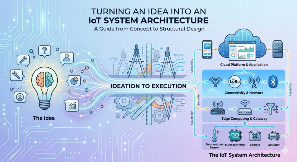
IoT system architecture serves as the foundational blueprint for any connected product, outlining how hardware, software, networks, and data interact to deliver value. It transforms abstract concepts into tangible, operable systems by defining components, interfaces, and data flows. A well-designed IoT architecture design ensures reliability, efficiency, and adaptability, preventing costly rework during later development stages.
Architecture is the backbone of successful IoT product development because it bridges the gap between ideation and execution. Poor architecture can lead to scalability bottlenecks, security vulnerabilities, or integration failures, while a robust one enables seamless growth from prototype to production. This article builds on the architecture stage in [Internal Link: The Complete IoT Product Development Roadmap: From Idea to Scalable Deployment], providing a deeper dive into converting validated ideas into structured IoT system blueprints.
Here, we’ll explore the systematic process of designing an IoT system, focusing on engineering principles to create scalable, secure architectures. Whether you’re an embedded engineer, solution architect, or startup founder, this guide emphasizes practical steps to turn user problems into comprehensive IoT solution architectures.
here are some usefull links for IoT System Architecture
Architecture of Internet of Things (IoT)
Unpacking IoT Architecture: Layers and Components Explained
From Problem Statement to System Requirements
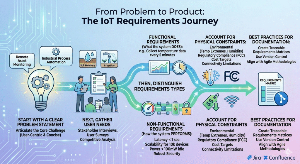
The journey from an IoT product idea to a solid architecture begins with a clear problem statement. Start by articulating the core challenge your system addresses—such as monitoring remote assets or automating industrial processes. This statement should be concise, user-centric, and free of assumptions, drawing from market validation discussed in the broader IoT product development roadmap.
Next, translate user needs into technical requirements. Conduct stakeholder interviews, user surveys, and competitive analysis to identify must-have features. For instance, if the idea involves smart agriculture, requirements might include soil moisture detection and automated irrigation triggers.
Distinguish between functional and non-functional requirements. Functional ones describe what the system does, like “collect temperature data every 5 minutes.” Non-functional requirements cover how it performs, such as latency under 1 second for real-time alerts, scalability to handle 10,000 devices, security against unauthorized access, and power consumption below 100mW in idle mode.
Account for constraints early: environmental factors like temperature extremes or humidity, regulatory compliance (e.g., FCC for RF emissions), cost targets per unit, and connectivity limitations in remote areas. These shape design choices and prevent surprises.
Best practices for documentation include using tools like Jira or Confluence to create traceable requirement matrices. Version control ensures changes are tracked, aligning with agile methodologies. This structured approach sets the stage for effective IoT architecture design, reducing ambiguity in subsequent layers.
A professional corporate infographic titled “From Problem to Product: The IoT Requirements Journey” illustrates a five-stage process using a clean, flat design with a blue, green, and white color palette. It features stages for the core challenge, gathering needs, a requirements split (functional vs. non-functional), physical constraints, and final documentation with logos for Jira and Confluence.
Defining IoT System Layers
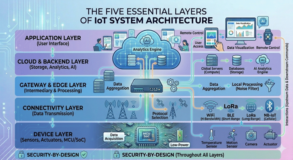
A layered approach simplifies complex IoT system design processes by breaking them into manageable components. This modular structure facilitates debugging, scaling, and maintenance in IoT device-to-cloud architectures.
The device layer encompasses sensors (e.g., temperature, motion), actuators (e.g., motors, valves), and the microcontroller unit (MCU) or system-on-chip (SoC). It handles data acquisition and basic processing, ensuring low-power operation for battery-constrained devices.
The connectivity layer manages data transmission using protocols like WiFi for high-bandwidth needs, Bluetooth Low Energy (BLE) for short-range pairing, LoRa for long-range low-power applications, or Narrowband IoT (NB-IoT) for cellular connectivity in urban settings. It focuses on reliable, secure links between devices and gateways.
The gateway or edge layer acts as an intermediary, aggregating data from multiple devices, performing local processing to reduce cloud latency, and handling protocol translations. For example, it might filter noise from sensor readings before upstream transmission.
The cloud or backend layer processes, stores, and analyzes data at scale. It includes servers for computation, databases for storage, and services for AI-driven insights, enabling global access and integration with enterprise systems.
Finally, the application layer provides user interfaces via web or mobile dashboards, allowing data visualization, remote control, and alerts. Interactions flow bidirectionally: data upstream from devices to apps, and commands downstream.
Each layer’s responsibilities—data handling, processing, and communication—must be clearly defined to ensure seamless interactions, forming a cohesive IoT product architecture.
Creating the System Block Diagram
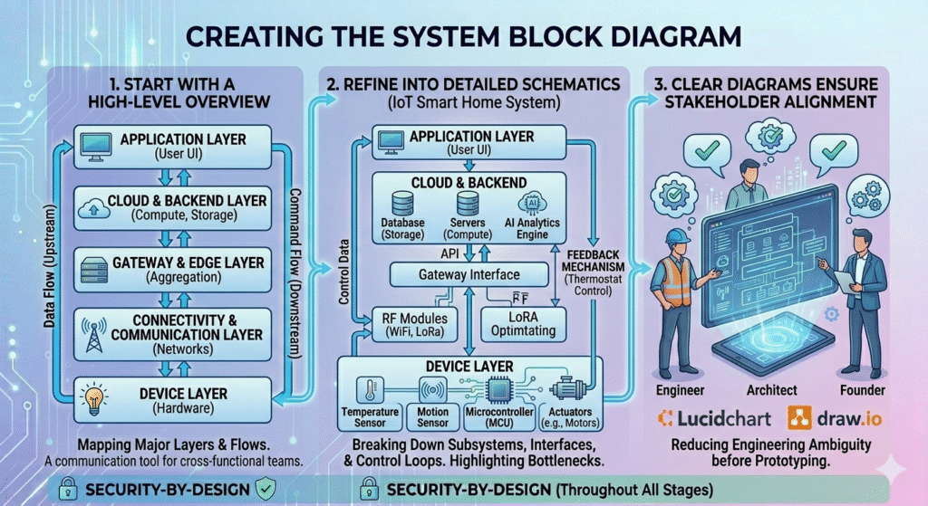
System block diagrams visualize the IoT system architecture, providing a high-level overview that evolves into detailed schematics. They map components, data flows, and interfaces, serving as a communication tool for cross-functional teams.
Start with a high-level diagram showing major layers: devices connected via networks to edge gateways, then to cloud services, and finally to user applications. Use arrows to indicate data flows, such as sensor data upstream and control commands downstream.
Refine into detailed diagrams by breaking down subsystems. For an IoT smart home system, depict MCU interfacing with sensors, RF modules for connectivity, and APIs for cloud integration. Include control loops, like feedback mechanisms for thermostat adjustments.
Clear diagrams reduce engineering ambiguity by highlighting potential bottlenecks, such as single points of failure in data paths. Tools like Lucidchart or Draw.io facilitate creation, ensuring stakeholders align on the IoT system design process before prototyping.
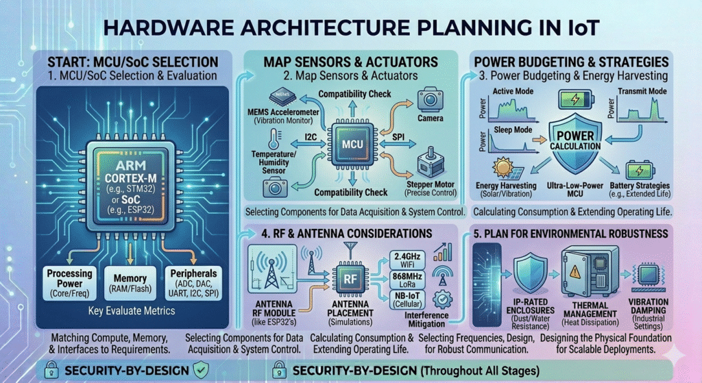
Hardware Architecture Planning
Hardware planning in IoT architecture design begins with MCU or SoC selection. Evaluate based on processing power (e.g., ARM Cortex-M for low-power apps), memory (RAM/Flash), and peripherals (ADC for sensors). For example, choose ESP32 for integrated WiFi/BLE.
Map sensors and actuators to requirements: use MEMS accelerometers for vibration monitoring or stepper motors for precise control. Ensure compatibility with MCU interfaces like I2C or SPI.
Power budgeting is critical—calculate consumption for active, sleep, and transmit modes. Implement battery strategies, such as energy harvesting or ultra-low-power MCUs, to extend life in remote deployments.
RF and antenna considerations include signal strength, range, and interference mitigation. Select antennas matching frequency bands (e.g., 2.4GHz for WiFi) and conduct simulations for optimal placement.
Plan for environmental robustness: use IP-rated enclosures for dust/water resistance, thermal management for heat dissipation, and vibration damping in industrial settings. This ensures the hardware foundation supports scalable IoT product architecture.
Firmware Architecture Design
Firmware architecture provides the software backbone for devices in an IoT system. Adopt a modular structure with separate modules for sensor drivers, communication stacks, and application logic, enabling easier updates and reuse.
Compare RTOS (Real-Time Operating System) like FreeRTOS for multitasking in complex systems versus bare-metal for simple, deterministic applications. RTOS handles task scheduling and synchronization, ideal for time-sensitive operations.
Manage tasks with priorities—e.g., high for interrupt handling of critical events like alarms. Integrate communication stacks modularly, supporting protocols without bloating code.
Incorporate error handling: use watchdog timers for resets and fail-safe modes to revert to safe states during faults. This design enhances reliability in IoT device-to-cloud architectures.
For authoritative guidance on RTOS, refer to the FreeRTOS documentation.
Connectivity and Communication Architecture
Selecting protocols is key in connectivity architecture. MQTT suits publish-subscribe models for efficient, low-bandwidth messaging; HTTP for RESTful APIs in web-integrated systems; CoAP for constrained devices in UDP-based networks.
Implement QoS (Quality of Service) levels in MQTT to ensure data reliability—e.g., QoS 2 for guaranteed delivery in critical applications. Balance edge vs. cloud processing: perform anomaly detection at the edge to minimize latency and bandwidth.
Consider network scalability: design for mesh topologies in BLE or hierarchical structures in LoRa to support growing device fleets.
For MQTT details, consult the MQTT specification.
Cloud and Backend Architecture
Cloud architecture starts with device provisioning: use services like AWS IoT Core for secure onboarding via unique identities and certificates.
Design databases for time-series data, such as InfluxDB or Amazon Timestream, optimized for high-ingress IoT streams.
API design includes REST or GraphQL endpoints with OAuth2 authentication flows for secure access.
Real-time processing pipelines leverage stream processors like Apache Kafka for handling live data.
Scalability strategies involve auto-scaling groups and load balancers to manage traffic spikes.
Explore AWS IoT documentation for implementation examples.
Security-by-Design Architecture
Embed security from the start: implement secure boot with hardware trust anchors like TPM chips to verify firmware integrity.
Use TLS 1.3 for encryption, managing certificates via automated rotations.
Adopt authentication models like JWT for devices and RBAC for users.
Secure OTA (Over-The-Air) updates with signed binaries and rollback capabilities.
Conduct basic threat modeling using STRIDE to identify risks like spoofing or tampering.
Reference NIST guidelines on IoT security for best practices.
Scalability and Future-Proofing
Design for scale by architecting microservices in the cloud, allowing independent scaling of components.
Plan modular expansions: use standardized interfaces for adding new sensors without redesign.
Firmware upgrade pathways include delta updates to minimize data usage.
Implement cloud auto-scaling and geographic redundancy for high availability.
This ensures the IoT system architecture evolves with business needs.
Common IoT Architecture Mistakes
Overengineering early inflates costs—start minimal and iterate based on requirements.
Ignoring power constraints leads to short battery life; always model consumption profiles.
Lacking OTA strategies hinders post-deployment fixes, exposing systems to vulnerabilities.
Weak cybersecurity planning invites breaches; integrate threat modeling from day one.
Poor documentation and no version control cause team misalignments; use Git for all artifacts.
Avoid these to streamline your IoT system design process.
Connection to the Full Roadmap
Architecture decisions ripple through the IoT product development lifecycle. They influence MVP prototyping by defining minimal viable features, cost estimation via component selections, certification compliance (e.g., CE marking), manufacturing scalability, and lifecycle management through updates.
A strong architecture minimizes risks in scaling and maintenance phases. For the complete context, explore [Internal Link: The Complete IoT Product Development Roadmap: From Idea to Scalable Deployment].
Related topics include The Complete IoT Product Development Roadmap: From Idea to Scalable Deployment
IoT Product Lifecycle Explained
This reinforces structured architecture’s role in overall success.
FAQ
What is IoT system architecture?
IoT system architecture is the structured blueprint defining how devices, networks, cloud services, and applications interact to form a connected ecosystem. It encompasses layers from hardware to software, ensuring scalability, security, and efficiency in IoT product architecture.
How do you design an IoT architecture?
Designing an IoT architecture starts with defining requirements, layering components (device, connectivity, edge, cloud, application), creating block diagrams, and planning hardware/firmware. Incorporate security and scalability to convert ideas into robust IoT system blueprints.
What are the layers of IoT architecture?
The layers include the device layer for sensors and MCUs, connectivity for protocols like WiFi or LoRa, edge/gateway for local processing, cloud/backend for data management, and application for user interfaces. Each handles specific responsibilities in IoT device-to-cloud architectures.
What is the difference between IoT architecture and IoT product design?
IoT architecture focuses on the system’s structural blueprint, including layers and data flows, while IoT product design encompasses broader aspects like user experience, aesthetics, and market fit. Architecture is a core subset enabling effective product realization.
How does architecture affect IoT scalability?
IoT architecture affects scalability by enabling modular components, auto-scaling cloud resources, and efficient protocols. Poor design causes bottlenecks, while thoughtful IoT solution architecture supports growth from hundreds to millions of devices without major overhauls.
What protocols are best for IoT communication architecture?
MQTT is ideal for lightweight, reliable messaging; CoAP for constrained environments; HTTP for web integrations. Selection depends on bandwidth, reliability, and power needs in your IoT system design process.
Why is security important in IoT architecture design?
Security prevents breaches in connected ecosystems. Incorporating secure boot, encryption, and threat modeling in IoT architecture design protects data and devices, ensuring trust and compliance throughout the product lifecycle.
Conclusion
Converting an IoT idea into a robust system architecture requires a methodical approach: from requirements gathering to layered design, diagramming, and planning for hardware, firmware, connectivity, cloud, security, and scalability. This structured thinking minimizes risks and maximizes efficiency.
Architecture decisions profoundly impact scalability, security, cost, and long-term viability, forming the core of successful deployments. By following these steps, engineers and architects can build resilient IoT systems.
To contextualize this within the full development journey, delve into [Internal Link: The Complete IoT Product Development Roadmap: From Idea to Scalable Deployment]. As a leading resource in IoT system and product development, we empower technical professionals with actionable insights for innovation.